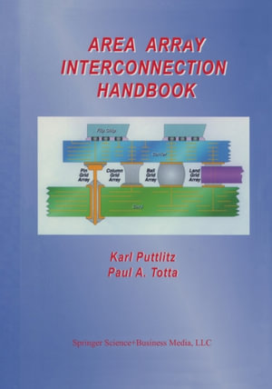
Area Array Interconnection Handbook
By: Karl J. Puttlitz, ?Paul A. Totta
eText | 6 December 2012 | Edition Number 1
At a Glance
eText
$84.99
or
Instant online reading in your Booktopia eTextbook Library *
Why choose an eTextbook?
Instant Access *
Purchase and read your book immediately
Read Aloud
Listen and follow along as Bookshelf reads to you
Study Tools
Built-in study tools like highlights and more
* eTextbooks are not downloadable to your eReader or an app and can be accessed via web browsers only. You must be connected to the internet and have no technical issues with your device or browser that could prevent the eTextbook from operating.
ISBN: 9781461513896
ISBN-10: 1461513898
Published: 6th December 2012
Format: PDF
Language: English
Publisher: Springer Nature
Edition Number: 1
You Can Find This eBook In
This product is categorised by
- Non-FictionEngineering & TechnologyElectronics & Communications EngineeringElectronics EngineeringCircuits & Components
- Non-FictionEngineering & TechnologyIndustrial Chemistry & Manufacturing Technologies
- Non-FictionEngineering & TechnologyEnvironmental Science
- Non-FictionEngineering & TechnologyEnergy Technology & EngineeringElectrical Engineering
- Non-FictionScienceBiology, Life SciencesLife Sciences in GeneralEcological Science


